- 您现在的位置:买卖IC网 > Sheet目录1204 > CSIX-LEV1-O4-N1 (Lattice Semiconductor Corporation)INTERFACE IP CSIX LEVEL 1 ORCA 4
�� �
�
�Lattice� Semiconductor�
�Detailed� Register� Descriptions� (Continued)�
�CSIX� Level� 1� IP� Core� User’s� Guide�
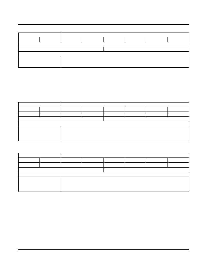
�Address:� 0x805C�
�Name:� Out_Cntrl_Hi_Watermark_0�
�D7�
�D6�
�D5�
�D4�
�D3�
�D2�
�D1�
�D0�
�OBC_HI_WMARK_0�
�Default� value:� 0x3f�
�Description:�
�OBC_HI_WMARK_0�
�Mode:� Read/Write�
�Channel� 0,� high� watermark� for� outbound� control� FIFO.� This� value� represents� the� number� of�
�FIFO� words� (4� bytes)� that� assert� the� FIFO� high� watermark.� When� the� number� of� words� in� the�
�FIFO� exceeds� this� value,� the� FIFO’s� PARTIAL_FULL� signal� asserts.�
�Watermark� registers� for� channels� 1� through� 3� reside� at� locations� 0x8080� -� 0x811C� as� shown� in� the� register� map.�
�The� detailed� descriptions� for� these� register� are� the� same� as� shown� for� channel� 0� except� that� the� registers� control�
�their� associated� channel� instantiation.� For� brevity,� these� register� descriptions� are� not� shown.�
�Note� that� when� channel� aggregation� is� used,� the� watermark� settings� of� the� channel� with� highest� precedence� con-�
�trol� the� behavior� of� all� the� aggregated� FIFOs.� The� watermark� settings� of� the� lower� order� channels� have� no� affect� on�
�FIFO� operation.�
�Address:� 0x8140�
�Name:� FIFO� Under?ow� Error� Register�
�D7�
�—�
�D6�
�—�
�D5�
�—�
�D4�
�—�
�D3�
�UF_ERR_3�
�D2�
�UF_ERR_2�
�D1�
�UF_ERR_1�
�D0�
�UF_ERR_0�
�Default� value:� n/a�
�Description:�
�UF_ERR_N�
�Address:� 0x8144�
�Mode:� Clear� on� Read�
�When� high,� indicates� that� one� of� the� FIFOs� for� channel� N� experienced� an� under?ow� error.� The�
�associated� channel’s� FIFOs� should� be� ?ushed� to� guarantee� proper� operation� after� the� under-�
�?ow.� This� bit� clears� upon� reading.� If� the� stimulus� that� caused� the� error� is� removed,� then� the�
�error� bit� in� this� register� will� clear� after� reading.�
�Name:� FIFO� Over?ow� Error� Register�
�D7�
�—�
�D6�
�—�
�D5�
�—�
�D4�
�—�
�D3�
�OF_ERR_3�
�D2�
�OF_ERR_2�
�D1�
�OOF_ERR_1�
�D0�
�OF_ERR_0�
�Default� value:� n/a�
�Description:�
�OF_ERR_N�
�Mode:� Clear� on� Read�
�When� high,� indicates� that� one� of� the� FIFOs� for� channel� N� experienced� an� over?ow� error.� The�
�associated� channel’s� FIFOs� should� be� ?ushed� to� guarantee� proper� operation� after� the� under-�
�?ow.� This� bit� clears� upon� reading.� If� the� stimulus� that� caused� the� error� is� removed,� then� the�
�error� bit� in� this� register� will� clear� after� reading.�
�12�
�发布紧急采购,3分钟左右您将得到回复。
相关PDF资料
CSIX-PI40-O4-N1
INTERFACE IP CSIX TO PI40 ORCA 4
CT0805S14BAUTOG
VARISTOR 14VRMS 0805 SMD AUTO
CT1206K17G
VARISTOR 17VRMS 1206 SMD
CTB-B-B-15
CIRCUIT BREAKER ROCKER 15A SP BK
CU3225K17AUTOG2
VARISTOR AUTO 17VRMS 3225 SMD
CU3225K250G2K1
VARISTOR STD 250VRMS 3225 SMD
CV10-RP-M-0
CONN JACK STR COAXIAL SMD
CVM50XM
MEMBER MOD PIC12C508/PIC12C509
相关代理商/技术参数
CSIX-PI40-O4-N1
功能描述:输入/输出控制器接口集成电路 CSIX to PI40 RoHS:否 制造商:Silicon Labs 产品: 输入/输出端数量: 工作电源电压: 最大工作温度:+ 85 C 最小工作温度:- 40 C 安装风格:SMD/SMT 封装 / 箱体:QFN-64 封装:Tray
CSJ-100
制造商:GREENLEE TOOL CO 功能描述:Digital Open Jaw Clampmeter 制造商:Greenlee Textron Inc 功能描述:CLAMPMETER
CSJ-23
功能描述:EXTRACTION TOOL FOR SCS RoHS:否 类别:工具 >> 插入,抽取 系列:* 标准包装:1 系列:* 其它名称:0011-03-00080011-03-0008-E00110300080011030008-E11-03-0008-E1103000811030008-EQ4729393AT0980176A
CSJ32C1
制造商:未知厂家 制造商全称:未知厂家 功能描述:HC-49/US SMD Microprocessor Crystals
CSJ32C3
制造商:未知厂家 制造商全称:未知厂家 功能描述:HC-49/US SMD Microprocessor Crystals
CSJ32C5
制造商:未知厂家 制造商全称:未知厂家 功能描述:HC-49/US SMD Microprocessor Crystals
CSJ32E1
制造商:未知厂家 制造商全称:未知厂家 功能描述:HC-49/US SMD Microprocessor Crystals
CSJ32E3
制造商:未知厂家 制造商全称:未知厂家 功能描述:HC-49/US SMD Microprocessor Crystals